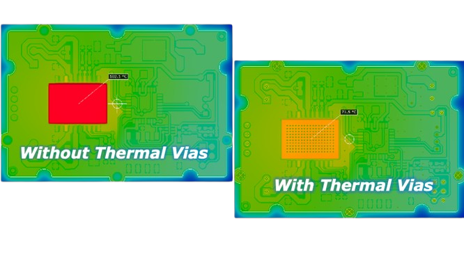
 In the fast-paced world of modern electronics, miniaturization and increasing power density are unstoppable trends. With circuits becoming ever more compact and powerful, the thermal management of electronic components has become a crucial challenge. A key component in this battle against heat is the Thermal Via.
This article will explore in detail what thermal vias are, why they are so important, how to design them effectively, and what considerations to keep in mind to maximize their effectiveness in heat dissipation on Printed Circuit Boards (PCBs).
What Are Thermal Vias?
Thermal vias are metallized holes (vias) strategically placed on a PCB, whose primary function is not the transmission of electrical signals, but the conduction of heat. They act as a thermal "bridge," transferring heat generated by high-power components (such as processors, voltage regulators, power LEDs, etc.) to cooler areas of the PCB, typically a ground plane or a larger copper area, which in turn can dissipate the heat into the environment or through a dedicated heat sink.
Imagine them as tiny "chimneys" that channel heat away from the source, preventing local overheating that could compromise the performance, reliability, and lifespan of the component or the entire circuit.
Why Are Thermal Vias Essential?
The need for thermal vias arises from several common thermal problems in PCBs:
- Component Thermal Overload: Many modern components generate a significant amount of heat during operation. Without effective dissipation, the internal temperature of the component can exceed the maximum specifications, leading to malfunctions or premature failure.
- High Power Density: With more components in smaller spaces, power density increases, concentrating heat in small areas.
- PCB Materials: PCB substrates (like FR-4) are excellent electrical insulators, but unfortunately also poor thermal conductors. Thermal vias provide a low thermal resistance path through these insulating layers.
- Reliability and Lifespan: Keeping components within their optimal operating temperature limits significantly extends their service life and the overall reliability of the system.
- Performance: Some components, such as LEDs, have performance directly related to operating temperature. Better thermal management can improve their light efficiency and color stability.
Designing Thermal Vias: Key Considerations
The effective design of thermal vias is not trivial and requires careful consideration of several parameters:
1. Placement and Distribution
- Under Dissipation Pads: Thermal vias should be placed directly under or around the thermal dissipation pads (Thermal Pad or Exposed Pad) of high-power components. This ensures the shortest and most direct path for heat transfer.
- Uniform Distribution: It is preferable to distribute the thermal vias uniformly under the thermal pad. A dense grid of vias can be more effective than a few large vias.
- Near the Edges of the Pad: Placing some vias along the edges of the pad can help capture heat that spreads laterally.
2. Dimensions (Diameter and Drilling)
- Hole Diameter: Typical hole diameters range from 0.3 mm (12 mil) to 0.5 mm (20 mil). Larger holes offer lower thermal resistance, but can reduce the available area for soldering and increase the risk of manufacturing problems (e.g., air trapping during reflow soldering).
- Outer Pad Diameter: The outer pad around the hole should be slightly larger than the hole itself to ensure a good contact and solderability area.
- Aspect Ratio: Although not directly related to thermal transfer, it is important to consider the aspect ratio (PCB thickness / hole diameter) for manufacturing.
3. Hole Finish: Tented, Non-Tented, Filled & Capped
The finish of thermal vias is a crucial and often overlooked aspect:
- Tented Vias (Covered by Solder Mask): The solder mask covers the hole and the via pad. This is the most common method and prevents unwanted short circuits. However, it can trap air during soldering, creating voids that reduce thermal efficiency.
- Non-Tented Vias (Not Covered by Solder Mask): The hole and pad remain exposed. This can improve the thermal connection, but increases the risk of short circuits with other elements or the formation of solder bridges. Rarely used under SMD components.
- Filled & Capped Vias: This is the most effective solution for thermal vias under high-power components. The holes are filled with a thermally conductive epoxy paste (or non-conductive if you just want to prevent voids) and then covered with a thin layer of copper (capping) and finally with the solder mask.
- Advantages: Eliminates air voids, provides a perfect planar surface for soldering (maximizing the thermal contact of the component), improves mechanical reliability and thermal dissipation.
- Disadvantages: Increases the cost and production time of the PCB.
4. Number of Vias
- Quantity: A larger number of thermal vias provides more paths for heat, reducing the overall thermal resistance. There is no fixed rule, but the goal is to saturate the available area under the component, while maintaining sufficient space for soldering.
- Copper/Via Area Ratio: It is important to balance the solid copper area (which is a good thermal conductor) with the area occupied by the vias.
5. Connection to the Ground/Copper Plane
Thermal vias must connect to a ground plane or a large copper area on the PCB. This plane acts as a heat "collector," distributing it over a larger surface for dissipation, possibly towards a heat sink or through convection/radiation. Ensure that the connection between the via and the ground plane is solid and wide.
6. Plating Thickness
A greater thickness of the copper plating inside the hole (barrel plating) improves the thermal conductivity of the via. PCB manufacturers specify standard thicknesses; if a greater thickness is required, this must be communicated.
Thermal Simulation and Best Practices
For the most critical projects, the use of thermal simulation software (such as ANSYS Icepak, Altium Designer with thermal analysis modules, or CFD tools) can provide accurate predictions of heat distribution and the effectiveness of the adopted solutions.
Some additional best practices:
- Windowed Pad: For components that require both electrical and thermal connections on the central pad (e.g., some Power MOSFETs), a "windowed" pad can be useful. This consists of an opening in the solder mask that exposes the underlying copper area for soldering, while the thermal vias are located within or around this area.
- Connection to Vias: Ensure that the copper around the component pad that connects to the vias is as wide as possible for good thermal transfer.
- Signal Routing: Avoid routing important signal traces between thermal vias, as they could obstruct the flow of heat or be affected by it.
Conclusion
Thermal vias are an essential and often underestimated design element in PCB thermal management. They are not just simple metallized holes, but rather crucial channels that allow high-power components to operate within safe temperature limits, ensuring reliability, durability, and optimal performance of the electronic system.
Careful design, which considers the placement, size, finish, and quantity of thermal vias, together with the use of thermal simulations for more complex projects, is essential for creating robust and thermally efficient PCBs. Investing time and resources in the correct implementation of thermal vias translates into a significant return in terms of stability and longevity of the final product.