As a PCB designer, you know how crucial accurate design is to ensure the functionality and manufacturability of a printed circuit board. Design rules are a set of specifications and limitations that guide the PCB layout, ensuring that the design can be manufactured efficiently and reliably. Ignoring these rules can lead to costly delays, rework, or even unusable boards.
This article explores the most common design rules that every PCB designer should know to optimize the production process, using the metric system.
Main Categories of Design Rules
- Clearance: Defines the minimum allowable distance between different conductive elements.
- Trace Width: Specifies the minimum and maximum width of conductive tracks.
- Pad Size: Determines the minimum and maximum dimensions of the pads.
- Vias and Drills: Regulates the minimum and maximum sizes of through-holes and pins.
- Planes: Defines the rules for creating and managing ground and power planes.
- Silkscreen: Establishes the minimum font sizes and line thicknesses for marking.
- Board Outline: Defines the shape and dimensions of the PCB.
Common and Critical Design Rules for Production (Metric System)
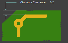
Minimum Clearance
The minimum clearance between conductive elements is essential to prevent short circuits. Typical values: 0.1 mm – 0.2 mm.
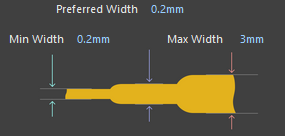
Minimum Trace Width
The minimum width is dictated by the current and manufacturing tolerances. Typical producible values: 0.1 mm – 0.15 mm.
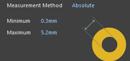
Minimum Pad Size
The dimensions must ensure a robust solder joint. Example: for a 0.8 mm hole, a pad of 1.2 mm – 1.5 mm.
Minimum Drill Size
The minimum diameter is limited by the manufacturer's equipment. Typical values: 0.2 mm – 0.3 mm.
Minimum Pad-to-Via Clearance
Minimum distance to avoid short circuits. Typical values: 0.1 mm – 0.15 mm.
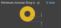
Minimum Annular Ring
Essential for a reliable electrical connection. Recommended typical values: 0.075 mm – 0.1 mm.
Thermal Relief
Reduces heat dissipation during soldering. Typical connection dimensions: width 0.15 – 0.2 mm, length 0.3 – 0.5 mm.
Rules for Ground and Power Planes
Minimum clearance from the edges (0.2 mm – 0.3 mm) and avoid isolated islands.
Rules for Silkscreen
- Minimum line width: 0.15 mm – 0.2 mm.
- Minimum character height: 0.8 mm – 1 mm.
- Avoid overlapping with pads.
Board Outline
 Precise definition with tolerances (typically +/- 0.1 mm – 0.2 mm) and details on chamfers or mounting holes.
The Importance of Communication with the Manufacturer
It is essential to actively communicate with the PCB manufacturer from the early stages of the project. Requesting their specific set of design rules is crucial.
CAD Tools and Design Rule Check (DRC)
Correctly configuring the DRC with the specific rules of the project and the manufacturer is essential to automatically identify and correct violations.
Conclusion
Compliance with design rules is crucial for manufacturable and reliable PCBs. Communication with the manufacturer and the use of the DRC are fundamental steps for the success of the project.
Contact me for a consultation on your next PCB!