In the complex world of printed circuit boards (PCBs), small but crucial elements play a fundamental role in ensuring electrical connectivity between the different layers: vias. Often underestimated, vias are conductive holes that allow signals and power to "travel" vertically through the multilayer PCB. Understanding the different types of vias and their applications is essential for a PCB designer to create efficient, reliable, and high-performance designs.
What Exactly Are Vias?
Imagine a multilayer PCB as a multi-layered cake, where each layer contains circuits and components. Vias are like metallized "bridges" that electrically connect these layers. Without vias, each layer would remain isolated, making it impossible to create complex circuits.
 A via is essentially a hole drilled through one or more layers of the PCB, which is then coated with a conductive material (usually copper). This metallization creates a low-resistance electrical path between the desired layers.
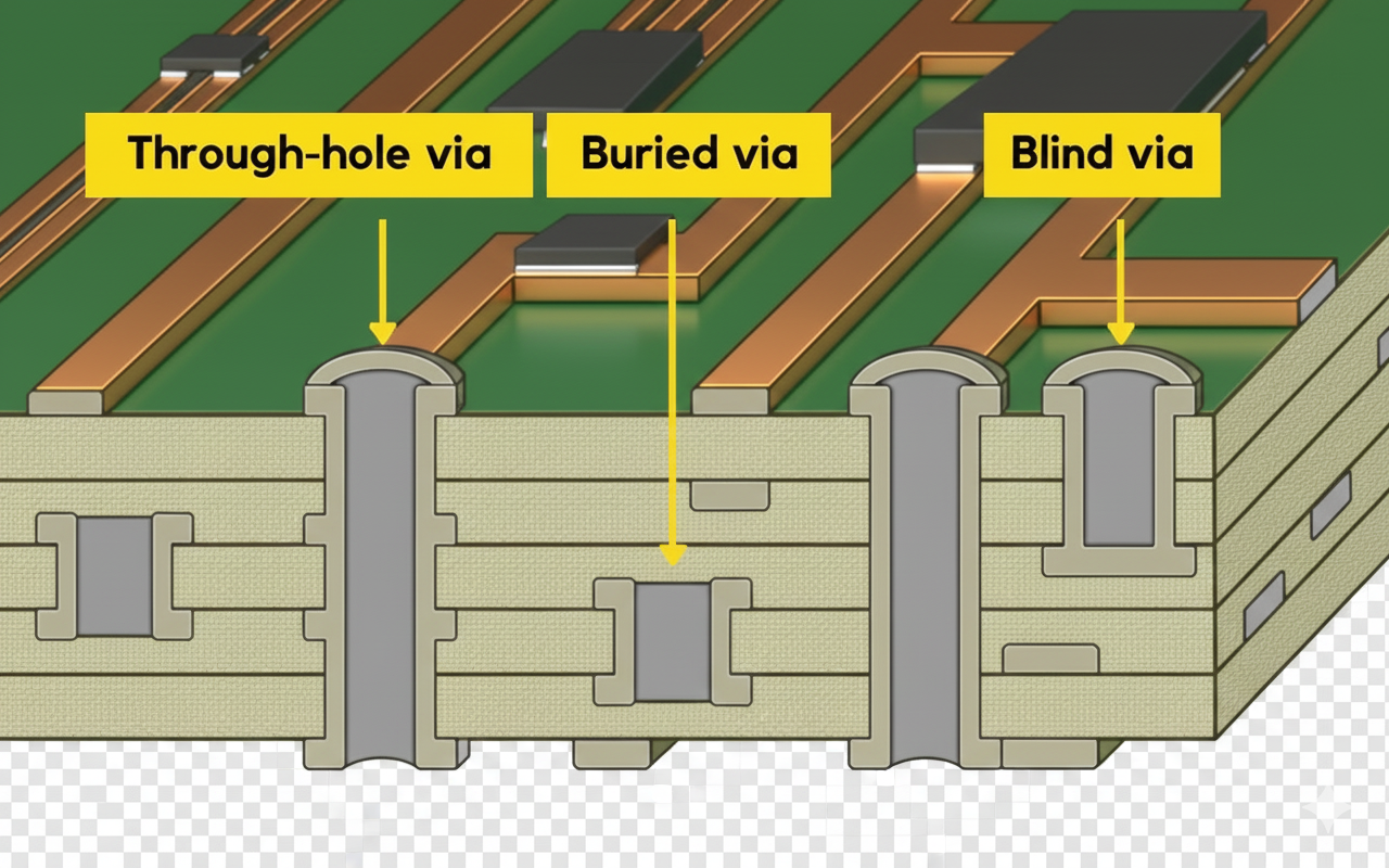
The Different Types of Vias:
Through-Hole Via
This is the most common and simplest type of via. A hole is drilled through all layers of the PCB, from the top surface to the bottom. They are easy to make and provide a robust connection, but they take up space on all layers, which can be a disadvantage in high-density designs.
Blind Via
As the name suggests, a blind via connects an outer layer to one or more adjacent inner layers, without passing through the entire PCB. They are useful for interconnecting specific layers, reducing clutter on other layers and improving component density on the surface. Their implementation is more complex than through-hole vias.
Buried Via
Buried vias connect two or more inner layers of the PCB and are not visible from the outer surfaces. They are essential for high-density designs as they do not take up space on the outer layers. Their fabrication requires more sophisticated processes and therefore they have a higher cost.
Microvia
These are extremely small vias (typically with a diameter of less than 150 µm) made with laser techniques. Microvias connect a surface layer to one or two adjacent inner layers. They are crucial for high-density interconnect (HDI) designs, allowing for finer routing and the placement of components with a very small pitch. They can be "stacked" (one on top of the other) or "staggered".
Via Filled/Plugged
In some applications, it is necessary to fill or plug vias, especially through-hole vias. This can be done with conductive or non-conductive material for several reasons:
- Void reduction: Prevents the formation of air bubbles during soldering processes.
- Flat surface: Creates a more uniform surface for component placement, especially for BGAs (Ball Grid Arrays).
- Thermal dissipation: Filling with thermally conductive material can improve heat management.
- Signal integrity: In high-speed applications, filling can help control impedance.
Practical Applications of the Different Types of Vias:
The choice of via type depends strictly on the project requirements:
- Simple and Low-Density Designs: Through-hole vias are often sufficient and are the most economical and simple solution.
- Medium-Density Designs with Space Constraints: Blind and buried vias become essential for interconnecting specific layers without taking up space on all layers.
- High-Density Designs (HDI): Microvias, often in stacked or staggered configurations, are the key to enabling complex routing and device miniaturization. They are commonly found in smartphones, tablets, and other compact electronic devices.
- Applications with High Thermal Requirements: Vias filled with thermally conductive material are used to dissipate heat from hot components to ground planes or heat sinks.
- High-Speed and High-Frequency Designs: Proper design and sometimes filling of vias are crucial to minimize impedance discontinuities and reduce signal reflections.
Important Considerations in Via Design:
During the PCB layout phase, it is essential to pay attention to several aspects related to vias:
- Hole and pad diameter: These must be chosen based on the manufacturer's capabilities and the current and signal requirements.
- Number of vias: An insufficient number of vias can cause connectivity and signal integrity problems, while an excessive number can increase costs and complicate the layout.
- Via placement: Their strategic placement is crucial to minimize trace length, reduce noise, and optimize electrical performance.
- Spacing between vias: It is necessary to respect the minimum spacing rules to avoid short circuits and manufacturing problems.
- Aspect Ratio: The ratio of the PCB thickness to the via hole diameter is a critical parameter for ensuring reliable metallization.
Conclusion:
Vias are essential elements that enable the functionality of multilayer PCBs. Understanding the different types of vias, their applications, and design considerations is fundamental for a PCB designer. Choosing the appropriate type of via for each specific situation significantly contributes to the quality, reliability, and performance of the final printed circuit board. A well-thought-out PCB design optimized in the use of vias results in more efficient and competitive electronic products.